PCB Concept
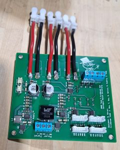
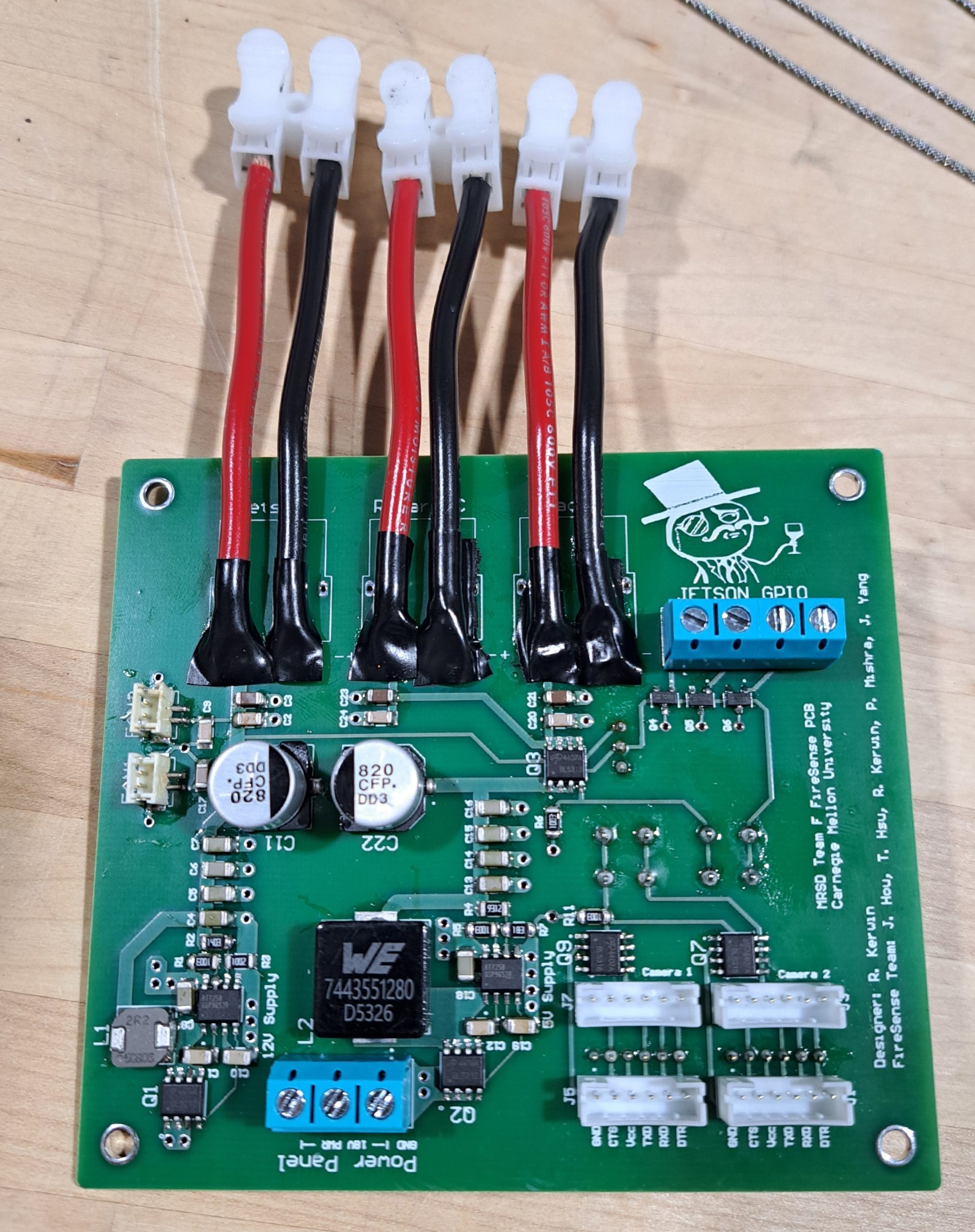
The PCB for Version 1 of the FireSense payload focused on power distribution and system debug information, and the final assembled version can be seen above. Below is the last conceptual design before moving forward with schematic development.
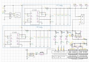
The payload is powered by an 18V battery, and so a PCB is needed to step down this voltage to 12V and 5V from a variable voltage between 15V and 21V (overcharged/undercharged battery). This is achieved through two RT7258GSP buck converters each configured for 12V and 5V outputs respectively. The 12V rail powers the Nvidia Jetson Orin AGX and two fans used to cool the Boson+ Thermal Cameras. The 5V rail powers the radar, radar capture card, and the LED debug panel.
PCB Schematic
The PCB was designed using Altium Professional Student License. We began by creating the schematic of our circuit. To do this effectively we needed to also have an in-depth understanding of the components that we would use. The strategy followed was to primarily design around the RT7258GSP buck converters, selecting the necessary resistors and inductors for proper function. Bulk & decoupling capacitors were added to stabilize the output of the signal.
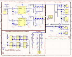
The debug board and functionalities of the PCB were then added, whith a UART pinout for each Thermal Camera and an array of 3 different color LEDs for programmable debugging.
PCB Layout creation in Altium
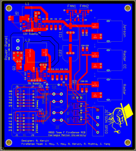
The layout of the PCB can be seen below. The red is the top layer routes, and the blue is the bottom layer power route and copper pour. When designing the board, there were a few considerations:
- Minimize right angle traces
- Adjust trace widths to ensure the traces can handle the current on its respective lines
- Add enough vias for the current –> ground
- Avoid the electromagnetic fields of the inductors
- Group debug features together to form the proper area for a debug panel
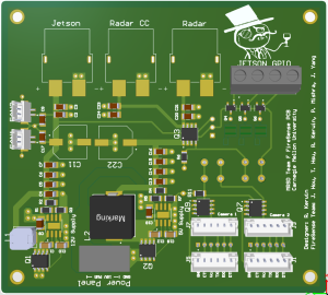
PCB 3D render of Layout
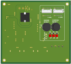
Through an online library called SnapEDA, we were able to procure many of the footprint and 3D models of many of the components. These models are able to be rendered in Altium, and so we are able to visualize the 3D space that the components take up on the board to avoid overlap. The front and back of this 3D render of the PCB layout can be seen below:
PCB Assembly
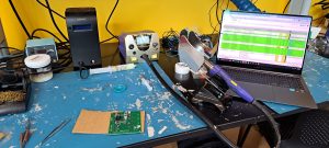
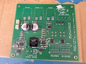
The assembly of the board was primarily conducted with thermal solder paste and a heat gun. This trivialized the surface mount assembly process compared to soldering with an iron. For the through hole components, the traditional approach with a solder iron was used in conjunction with plenty of solder flux. The photo below shows the assembly workstation. Pardon the poor ESD protections, as the PCB lab’s ground pads had been covered in solder paste and there was serious concern about bridging. This board is one of three, and so on future assemblies a better & cleaner mat will be used.